Full Adder 74HCxx Circuit
-
Concept of Operation
The full adder circuit performs binary addition on three one-bit numbers. It is distinguished from the half adder which adds two one-bit numbers. The full adder combines two half adders and adds an OR gate to the the circuit.
The circuit is called a full adder because the third bit is used to bring in the carry bit from a half adder or another full adder. The ability to integrate a carry-in bit enables multiple full adders to be chained together to build adders that can handle 4-bit, 8-bit and larger additions.
The full adder is implemented here using 74HCxx series high-speed CMOS digital logic ICs.
-
Schematic

-
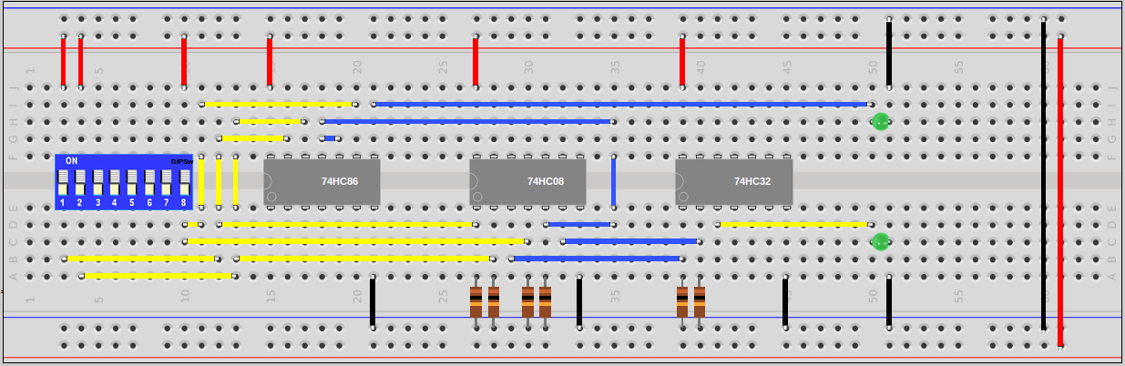
Breadboard Diagram
-
Parts
- SN74HC86 - Quad 2-Input XOR Gate IC (x1)
- SN74HC08 - Quad 2-Input AND Gate IC (x1)
- SN74HC32N - Quad 2-Input OR Gate IC (x1)
- 10K Resistor (x6)
- Green 5v LED (x2)
- 8 Position DIP Switch (x1)
(All parts for the project are available in our store.)
-
Truth Table
| Input |
Output |
| Carry In |
A |
B |
Sum |
Carry Out |
| 0 |
0 |
0 |
0 |
0 |
| 0 |
0 |
1 |
1 |
0 |
| 0 |
1 |
0 |
1 |
0 |
| 0 |
1 |
1 |
0 |
1 |
| 1 |
0 |
0 |
1 |
0 |
| 1 |
0 |
1 |
0 |
1 |
| 1 |
1 |
0 |
0 |
1 |
| 1 |
1 |
1 |
1 |
1 |
-
SN74HC08 Pinout

-
SN74HC32 Pinout
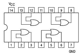
-
SN74HC86 Pinout

-
Notes on Implementation
- In the schematic the 8 position DIP switch appears as two devices and unused switches are not shown. Refer to the board diagram for placement of the DIP switches.
- Be mindful of the notch on the IC package which indicates proper orientation of the device.
- The schematic symbols for the IC logic gates with multiple gates per chip are noted with A, B etc. to designate the different gates on the same chip.
- The LEDs used in the project have a built in current limiting resistor eliminating the need for an external resistor to protect the device. This resistor is shown in the schematic as a resistor with the value “Lim” for completeness.
- The circuit was built and tested at 4.8 volts DC (4 AA NiMH rechargeable batteries). The 74HCxx series ICs are rated from 2 to 6 volts.
